A Mutable Log
A blog by Devendra Tewari
Project maintained by tewarid Hosted on GitHub Pages — Theme by mattgraham
Prototyping a PCB using LPKF ProtoMat S62
The last time I designed my own PCB, in 1995, I used parchment (butter) paper and stickers. The fabrication was contracted out to a third-party. Times have changed, we now have simple circuit design software such as Fritzing, and rapid PCB prototyping machines such as the LPKF ProtoMat S62. Though the latter doesn’t come cheap, it is totally worth it.
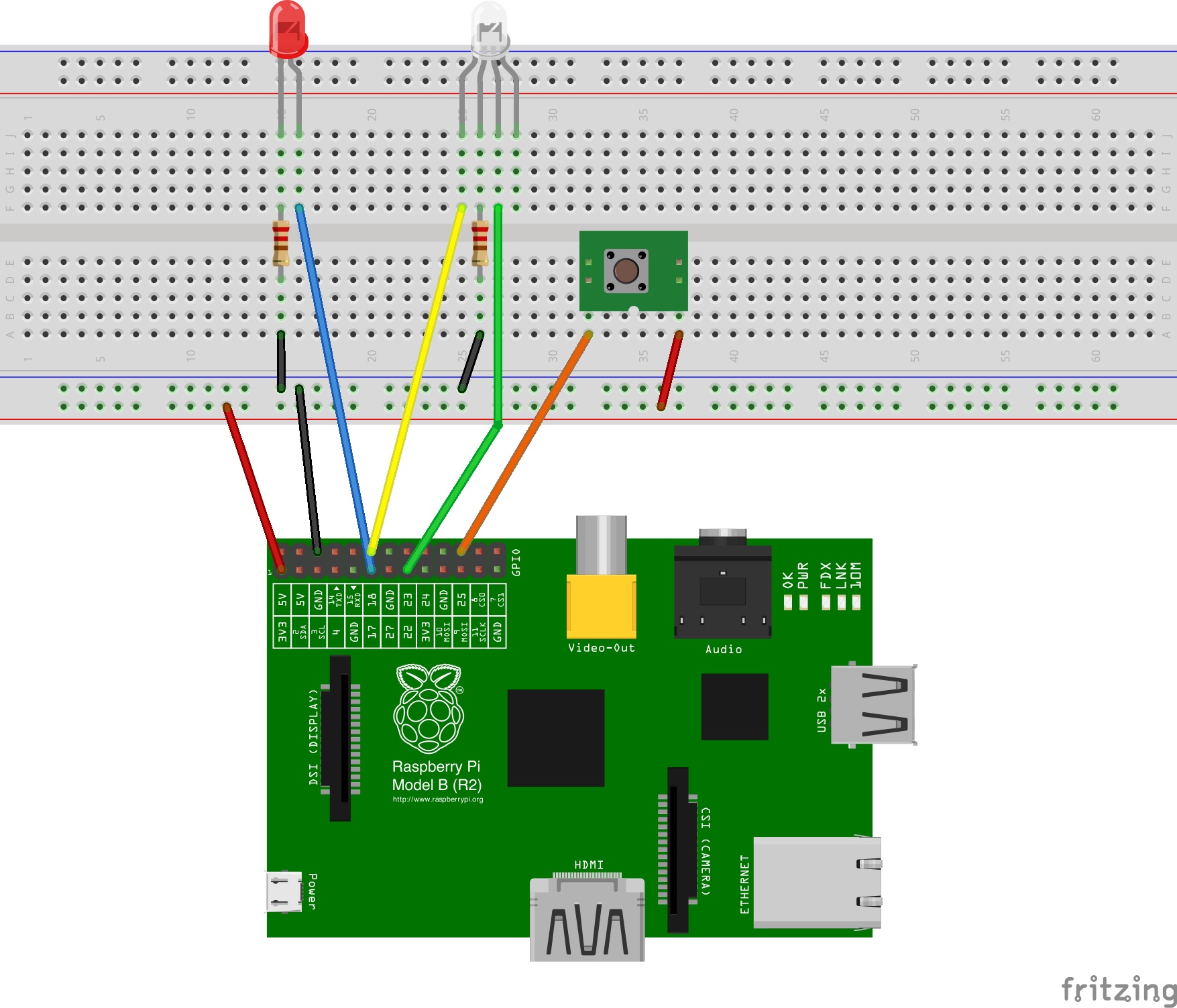
The PCB I designed is very simple, and contains only through-hole parts. It is a custom breakout for the Raspberry Pi Model B Rev 2. I found most components in the Fritzing library. The Raspberry Pi component was obtained from the Adafruit Fritzing library at GitHub (AdaFruit.fzbz).
This is how the breadboard view looks
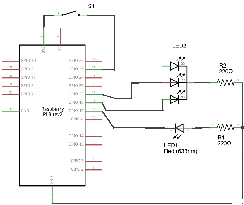
The schematic after some cleanup looks like this
I let Fritzing autoroute traces, and then fixed whatever issues its DRC (design rules checker) brought up.
The two-sided PCB after some work looks like this
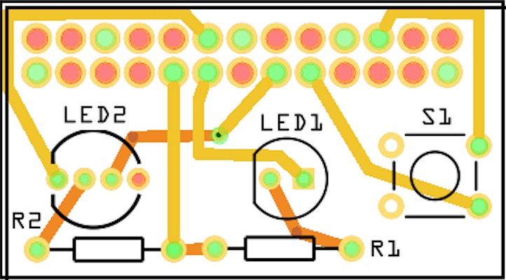
The prototyping environment lacks PTH (plated through hole) capability. Although holes are drilled, we are unable to deposit copper through holes and vias. To enable easier soldering, I moved traces leading away from the header to the top PCB layer. Since the header is placed on the bottom layer, I would only be able to solder its pins on the top layer.
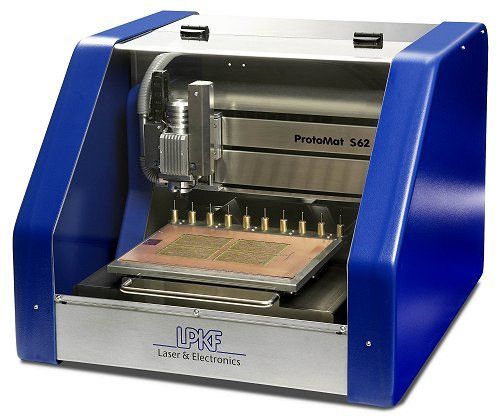
Milling was carried out by a colleague at work, who’s trained herself to use the ProtoMat S62 and its accompanying software such as CircuitCam and BoardMaster. She used the Gerber (RS-274X) files I exported using Fritzing.
This is the kind of machine that was used
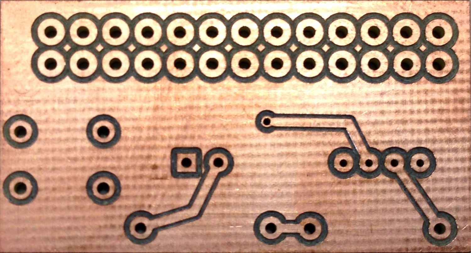
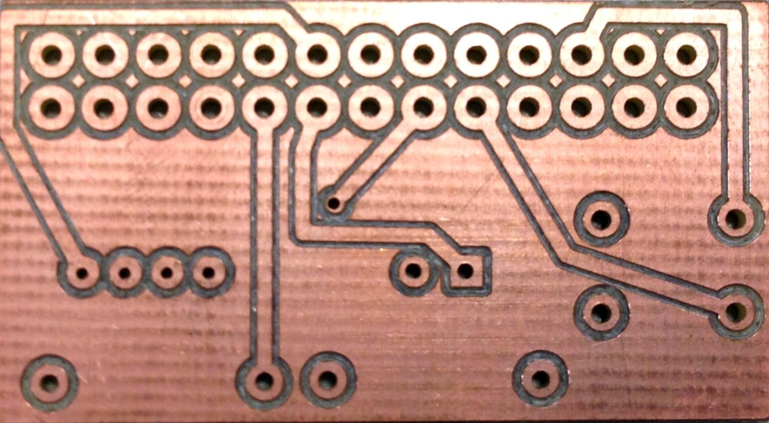
Here’s how the finished PCB looks (bottom layer appears first)
Here’s the PCB, with most components now soldered
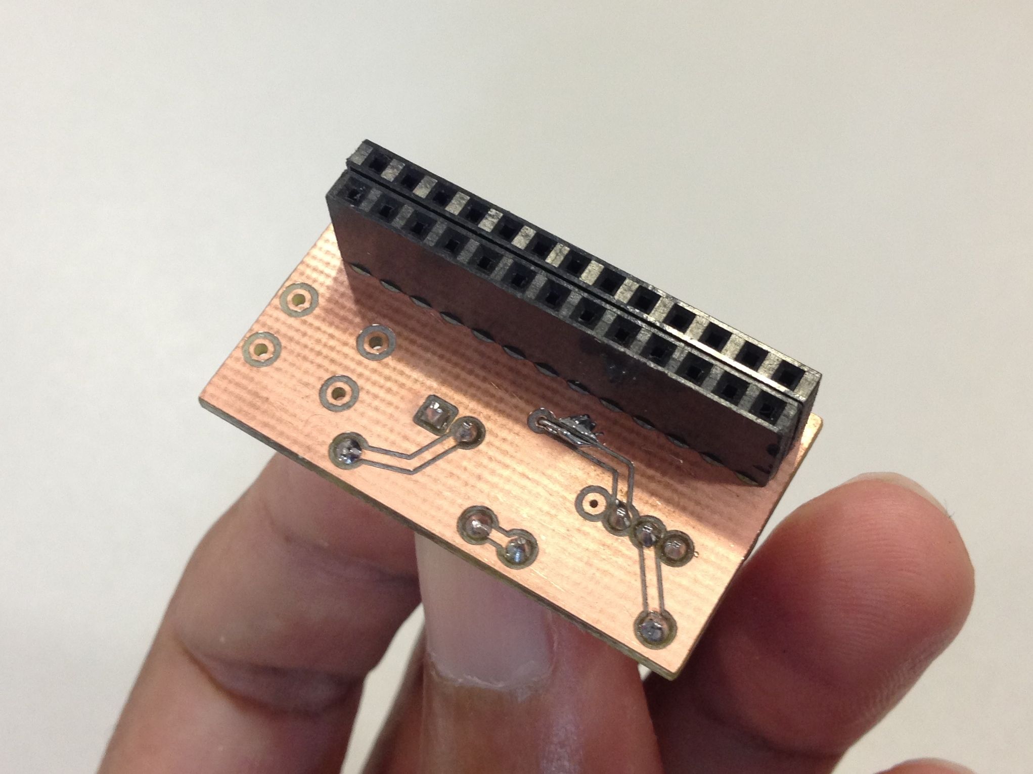
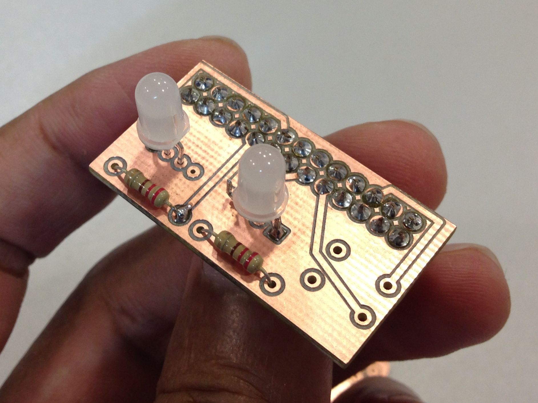
Some components are soldered on both sides because they pass signals from one layer to another. As mentioned earlier, we lack PTH capability.
I have a lot to learn about PCB designing and the ProtoMat S62, but it’s a start.